
The process of designing and manufacturing integrated circuits or chips is complex, involving multiple stages where faults can occur. Ensuring the reliability of chips is critical, as they are a key component in countless electronic devices and embedded systems. Comprehensive verification and testing strategies are required to catch faults early and confirm manufacturing quality. This article explores some key verification and testing techniques for vlsi design and vlsi circuits at various stages of the design flow.
Verifying the correctness of chip designs and thoroughly testing manufactured chips is crucial for identifying and eliminating defects. As chips continue to grow in complexity with smaller feature sizes, more sophisticated verification and testing methodologies are needed. Strategies implemented from early design concept to final fabrication and assembly can catch bugs and flaws before they become expensive problems. This allows reliability issues to be addressed proactively, reducing risk and ensuring a robust embedded system solution.
Simulation in the Design Stage
Verification of chip designs begins early, while they are still in the form of register transfer level (RTL) specifications. RTL descriptions model the digital circuit in terms of the flow of signals between hardware registers and the logical operations performed on them. Simulation tools can execute the RTL code and provide functional verification even before synthesis converts the design to gates. Popular logic simulators like ModelSim can check for incorrect functionality, protocol errors, timing issues, and other problems in the logic specifications. Constrained random verification explores a wide range of valid and invalid stimuli to uncover corner-case flaws. Formal verification mathematically proves properties about the design, like equivalence between two versions or the absence of deadlock conditions. Together, simulation techniques provide comprehensive verification to prevent bugs from manifesting after chips are fabricated.
Physical Verification after Synthesis
Following RTL simulation, synthesis transforms the logic design into an actual gate-level netlist suitable for implementation in silicon. The synthesized netlist undergoes physical verification to ensure it correctly implements the RTL functionality and meets manufacturing constraints. A layout versus schematic (LVS) check confirms the correspondence between the netlist and the physical layout geometry that will be used to fabricate the chip. Design rule checking (DRC) verifies that the layout adheres to geometric rules like minimum spacing between wires and allowed widths of transistors. These physical verification steps identify problems arising from synthesis or layout, so the netlist and layout can be corrected as needed.
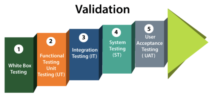
Testing Manufactured Chips
Once the design is verified and chips are manufactured, rigorous testing is conducted to catch any defects resulting from fabrication. Production testing screens for both catastrophic faults like open or short circuits as well as more subtle parametric faults that affect performance but not outright functionality. Common techniques include scan testing, which uses scan chains to deeply access internal circuit states; IDDQ testing to measure quiescent supply current and detect shorts; and functional testing, which applies vectors to exercise different modes of operation. Burn-in testing accelerates infant mortality failure by stressing chips at high temperatures and voltages to weed out marginal components. Automated test equipment equipped with probes tests key pins and interfaces. Rigorous testing at multiple levels ensures that VLSI circuits shipped to customers are as defect-free as possible.
In-field Monitoring for Wear-Out Issues
While pre-shipment testing targets manufacturing defects, reliability challenges can also arise after deployment in the field. In particular, integrated circuits are susceptible to electromigration, hot carrier injection, bias temperature instability, and other forms of degradation over time. In-field monitoring tracks performance metrics like timing delays and operating currents to detect signs of wear before they lead to functional failure. Strategies include built-in self-test circuitry, on-chip monitors and sensors, nuanced performance benchmarks, and out-of-band analytics of telemetry data. The goal is to obtain leading indicators of deterioration so proactive steps can be taken. This allows reliability risks to be managed throughout the operational lifetime of chips, enabling a robust embedded system solution.
Adopting a full-flow verification mindset
Delivering reliable, high-quality chips requires adopting verification strategies that span the entire development flow. Too often, verification is an afterthought or addressed too late once major design decisions have been made. The most effective approach is a full-flow verification mindset, validating correctness from the initial concept through RTL implementation, physical design, manufacturing, testing, and in-field operation. A continuous evaluation of reliability risks allows issues to be addressed at the earliest, most cost-effective stage. Mandating sign-offs and checklists along the way helps ensure verification completeness. As VLSI design complexity increases, diligent verification and testing at every step becomes mandatory to confirm robustness and achieve an effective embedded system solution.
Leveraging Automation and AI for Efficient Verification
As complexity rises, pure manual verification becomes infeasible. Automation and AI techniques can augment engineers to improve verification productivity. Tools apply intelligent test generation, results analysis, coverage closure, and formal methods. Machine learning models can be trained to classify design rule violations. By taking over repetitive tasks, automation amplifies and accelerates the expertise of human verification teams.
Importance of a Verification Plan
Any robust verification methodology requires comprehensive planning upfront. A verification plan identifies necessary activities, checks, and sign-offs for each design stage. Items like test benches, coverage goals, tools, metrics, and schedules are detailed. This upfront planning prevents critical verification tasks from being missed. The plan also allows for tracking progress and completion status throughout the project lifecycle.
Reusing verification assets
Verification and reuse are key for efficiency across projects. Verification intellectual property (VIP) encapsulates pre-built environments to test standard interfaces like PCIe or USB. Test suites, stimulus generators, coverage models, and other assets can be reused across chip projects. This amortizes the upfront investment in verification while increasing productivity. A library of modular verification building blocks minimizes redundant recreation of tests.
Conclusion
Ensuring chip reliability poses growing challenges as designs become more intricate. This requires evolving verification and testing techniques to keep pace. Early-stage simulation provides powerful bug hunting before cost commitments are made. Physical verification confirms the manufacturability of the design. Rigorous testing screens for defects and infant mortality in manufactured chips. And in-field monitoring helps manage deterioration over the product’s lifetime. Adopting a full-flow verification mindset strengthens reliability assurance across the complete VLSI circuit development process, enabling robust embedded system solutions. With chips becoming ubiquitous in modern devices and infrastructure, continued advances in verification and testing will be crucial for delivering dependable functionality.
FOR MORE INFORMATION VISIT OUR HOMEPAGE:


 7")


 12")